A project by Charles Singleton.
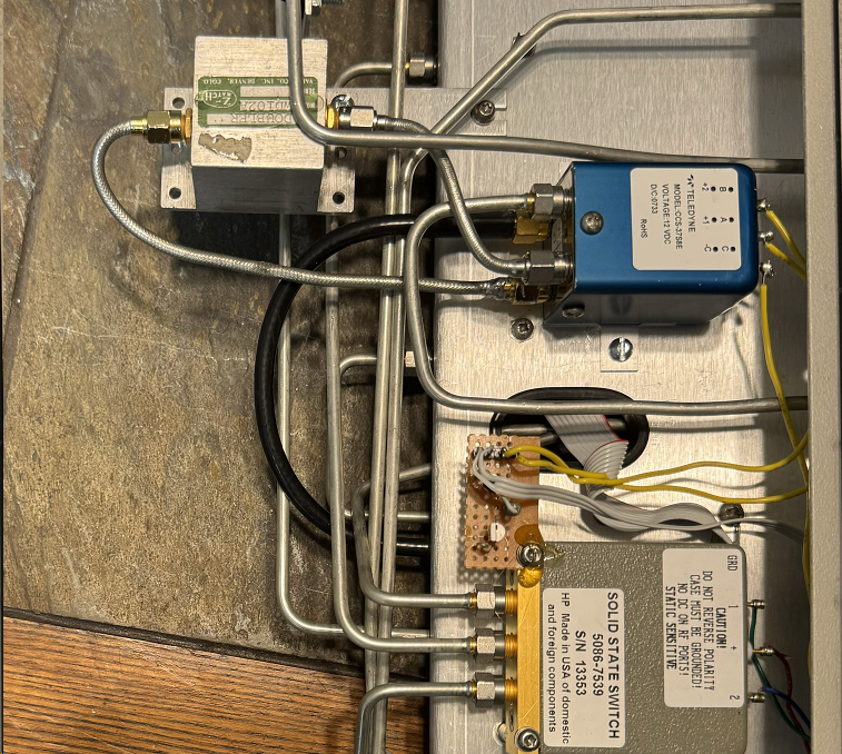
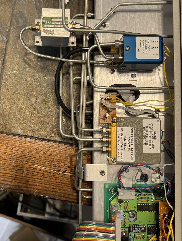
After obtaining a surplus HP 8753C Network Analyzer and HP 85046 3GHz test set on eBay, I decided to look out of curiosity to see what the differences were between my test set and a 6GHz 85047 unit. I learned that the 87053C analyzer would operate in the 6GHz mode with the 85047-test set. Option 006, 6GHz option is just a software feature of the 8753C. If the option isn’t installed, it can be installed from the front panel using the instructions here. After the option is installed, the 8753C will not switch to 6GHz unless it sees a 6GHz test set attached. Looking at the service manuals for both test sets reveals the differences. The 85047 contains 2 extra RF modules. A 4 port RF switch and a frequency doubler. Both of these modules can be had for less than $100 on eBay if you look around. There is no need to get the exact HP parts. I obtained a VARI-L WD102A Doubler on eBay for $15.00 that fits the bill, And a Teledyne CCS-37S8E 4-port switch I had on hand. Most 4 port RF switches with SMA connectors should work.
This is how the modules were mounted inside my 85046.
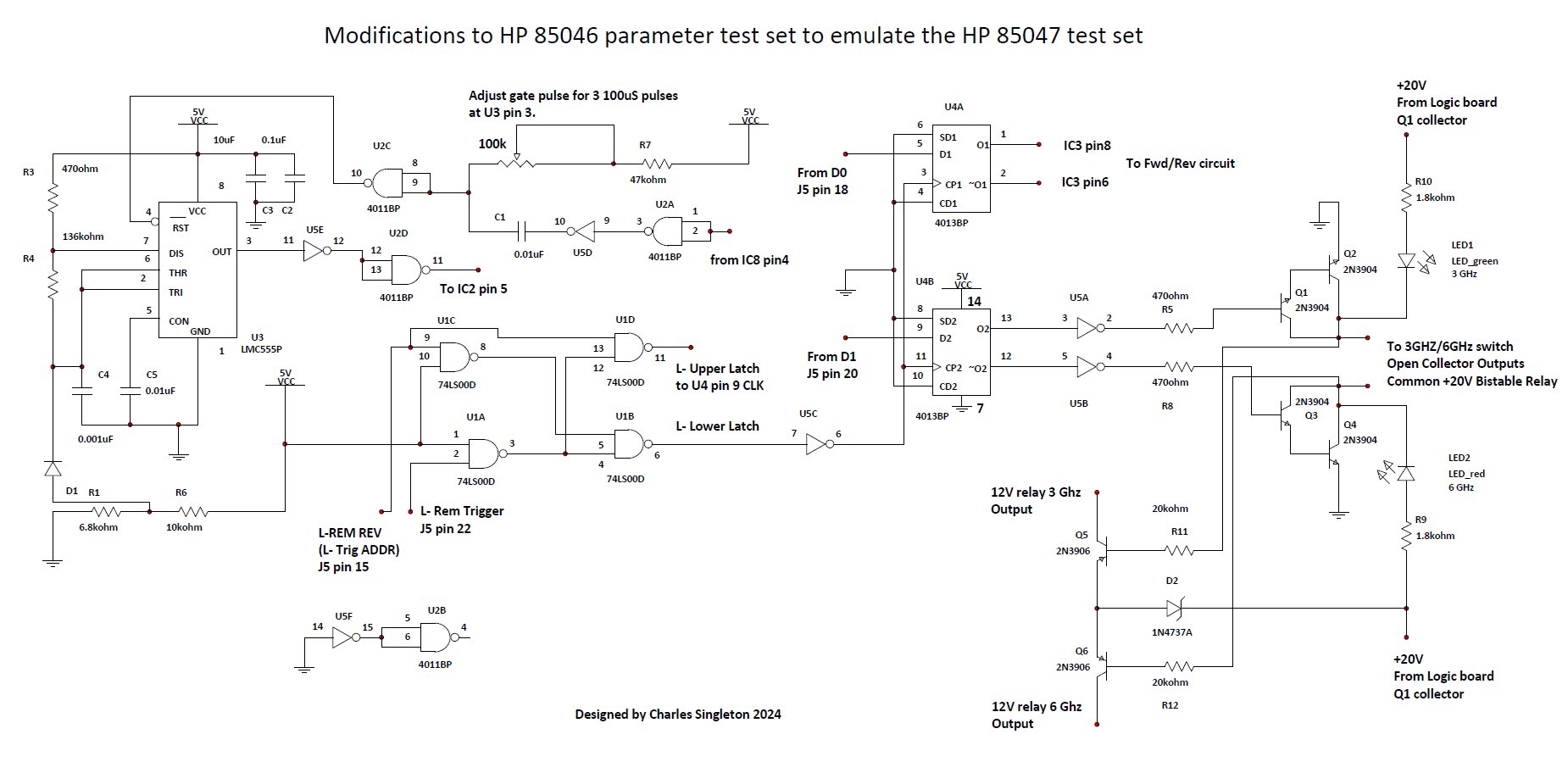
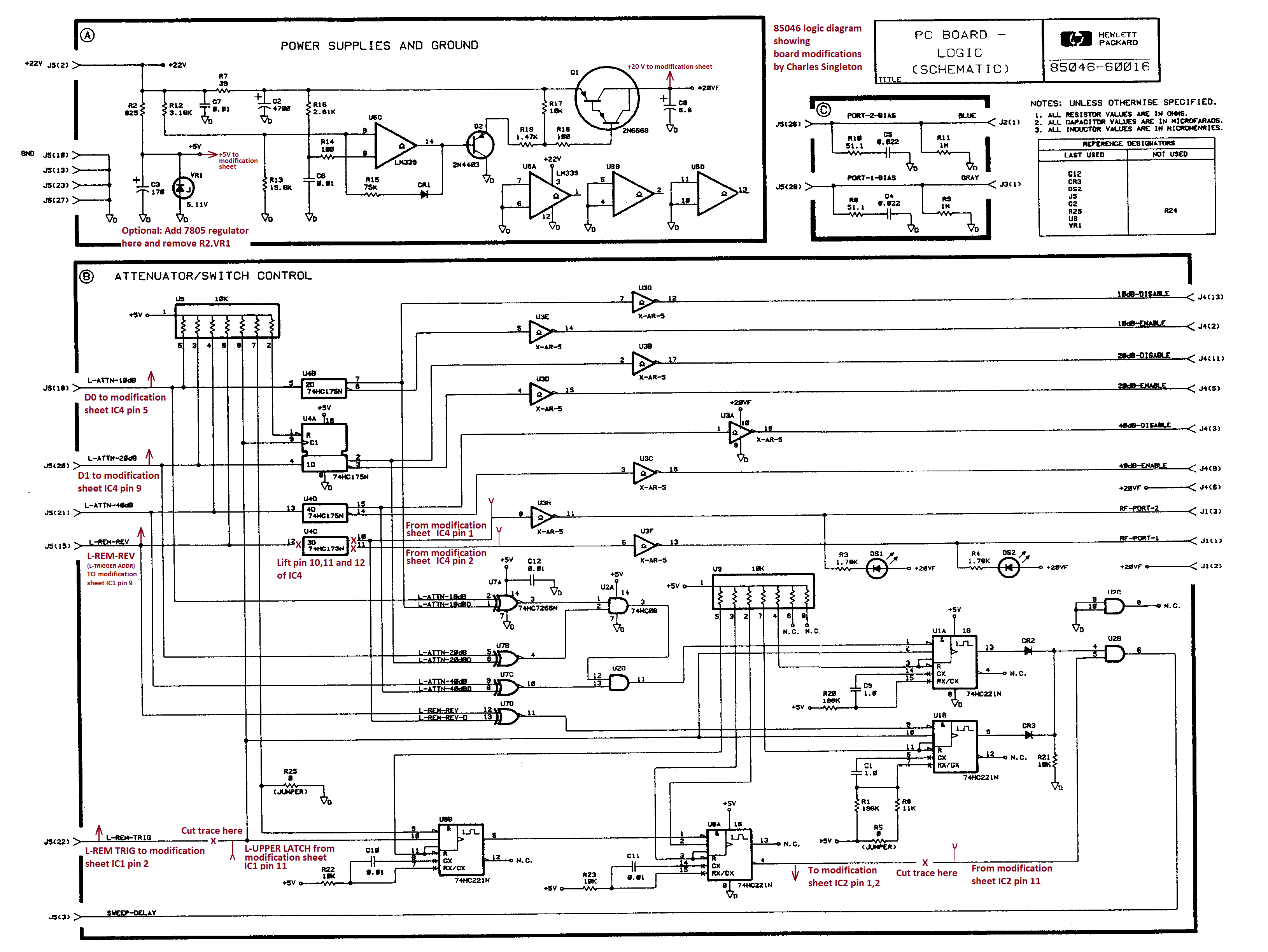
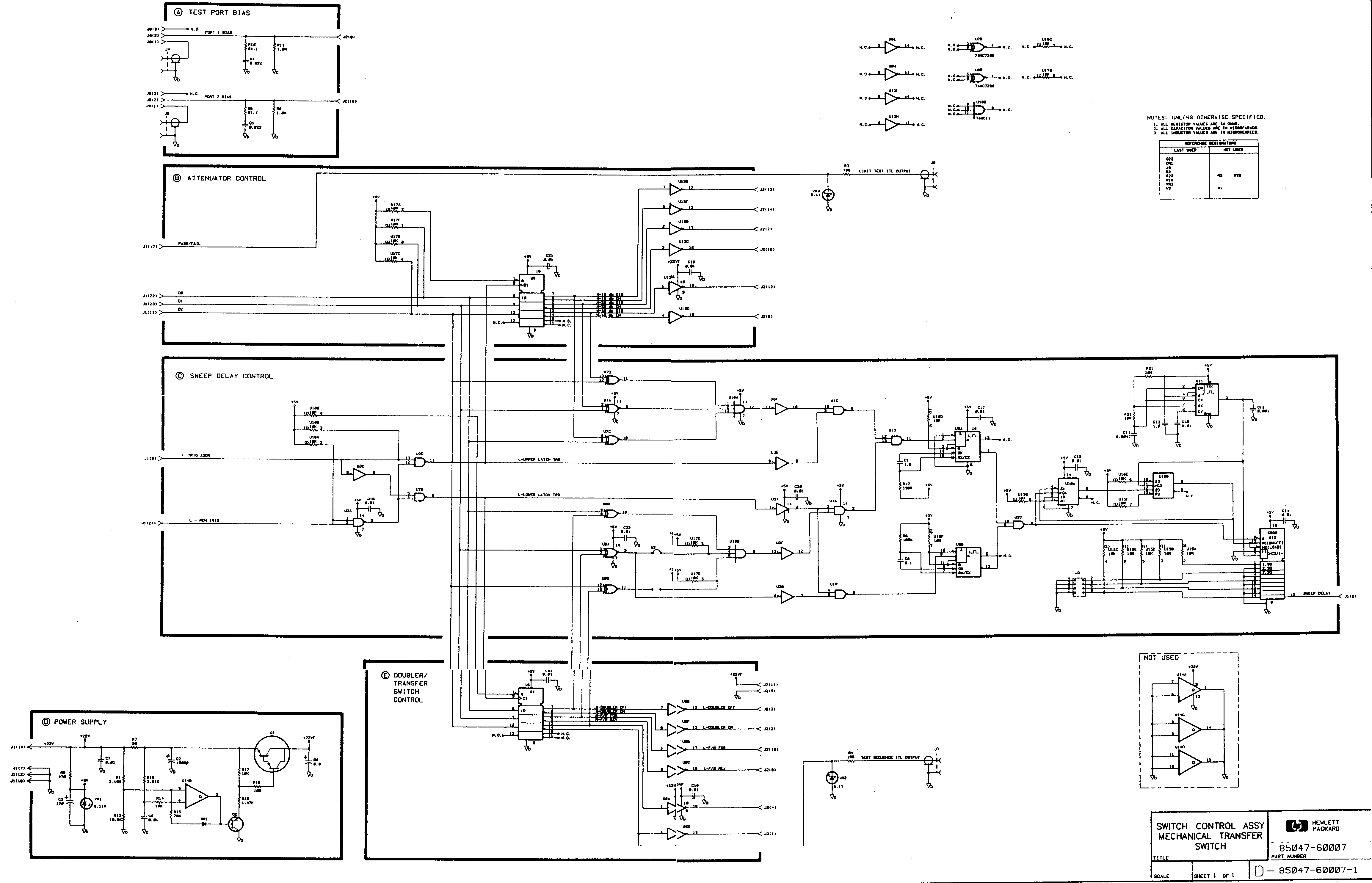
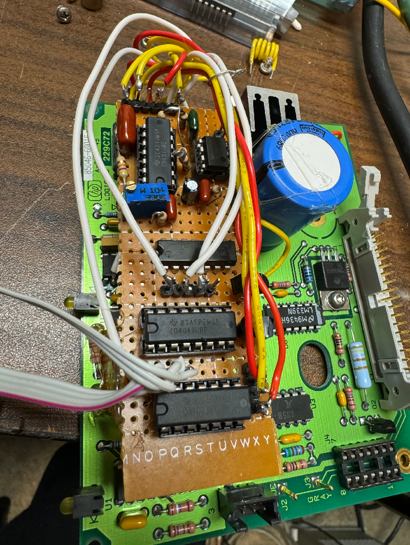
An additional circuit board was built that rides on top of the existing logic board. It contains a logic circuit that completes the needed signals, and controls the switches, attenuator and LEDs. See the MODIFICATION SCHEMATIC and the Original Logic Board here. Referring to the 2 schematics, you can see how the modification adds the additional pulses for the 8753C to identify the test set as an 85047 6 GHz set. All the features of the 85047 will be available as a result. Keep in mind that the Network analyzer will not send the proper signals until it receives the pulse train identifying the test set. The manuals explain this and give all the information needed to design a circuit to add the correct pulse train. See the manual excerpts below showing the differences between the 2 test sets.
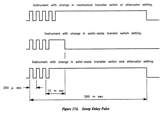
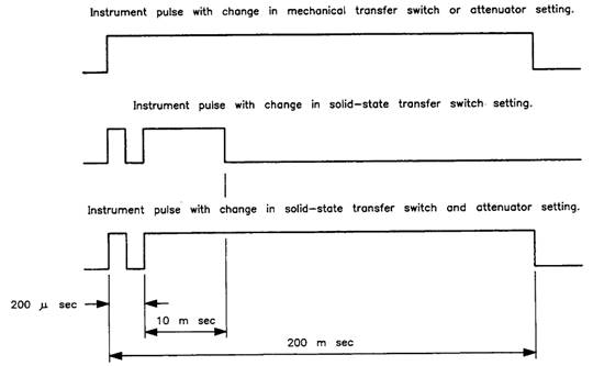
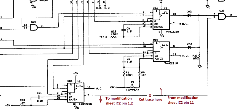
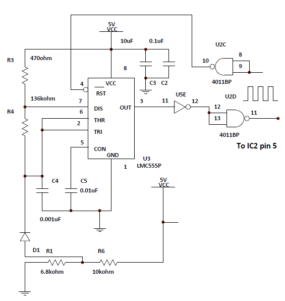
The modification adds 3 pulses each time we get a trigger, replacing the single 100 µSec pulse from the original sweep delay circuit. From the schematics below, it can be seen where I cut the trace between IC8 pin 4 and IC5 pin 5. Using the signal from U8 pin 4 of the existing logic board, I trigger a one shot to generate a gating pulse for the LMC555 astable multivibrator. The astable multivibrator then generates 3 pulses to be applied to U2 pin 5. This will tell the 8753C to make 6GHZ mode available, and to switch logic control mode to control an 85047 test set.
Following along with the MODIFICATION SCHEMATIC, we can discuss the pulse generator portion of the modification. The multivibrator consists of a CMOS style 555 timer chip gated by a second multivibrator. When pin 4 U3 is high, a continuous stream of 100 µSec pulses is generated. The gate length is about 550 µS so that lets 3 positive-going 100 µS pulses out on pin 3 that are later inserted into the sweep delay signal.
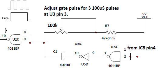
The gated multivibrator is shown below. U2C gates this on for about 550 µS each time there is a sweep. A low power version of the 555 is used, the LMC555P to keep power consumption very low. D1, R1 and R6 create an initial bias so the first pulse is not wider than the following ones. It takes longer to charge C4 the first time because the voltage starts at zero unless a bias network keeps a minimum voltage on C4. The output is double buffered before it goes out to IC2 pin 5 of the original logic board.
You may notice my choice of devices could be different, and some other devices may make more sense. You could follow this design and use the devices of choice to get the same logical outcome. My choices were made because I had these parts on hand. Many other parts could be utilized.
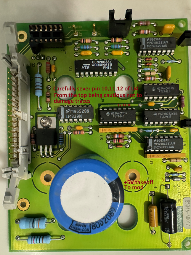
Below is a picture of an unmodified 85046 logic board from the top side. It shows the location of the most critical operation than has to be done to the board. Pins 10,11 and 12 of U4 have to be severed from the PC board and floated. I did this by using very small wire clippers to cut the pins loose from the chip body. Care must be taken not to damage traces. There are traces under the chip that can be damaged easily. If you should damage them, you can follow the schematic to run replacement wire connections. As an alternate to snipping the leads, you can completely desolder and remove the chip, bend up pins 10,11 and 12 then reinstall without those pins connected.
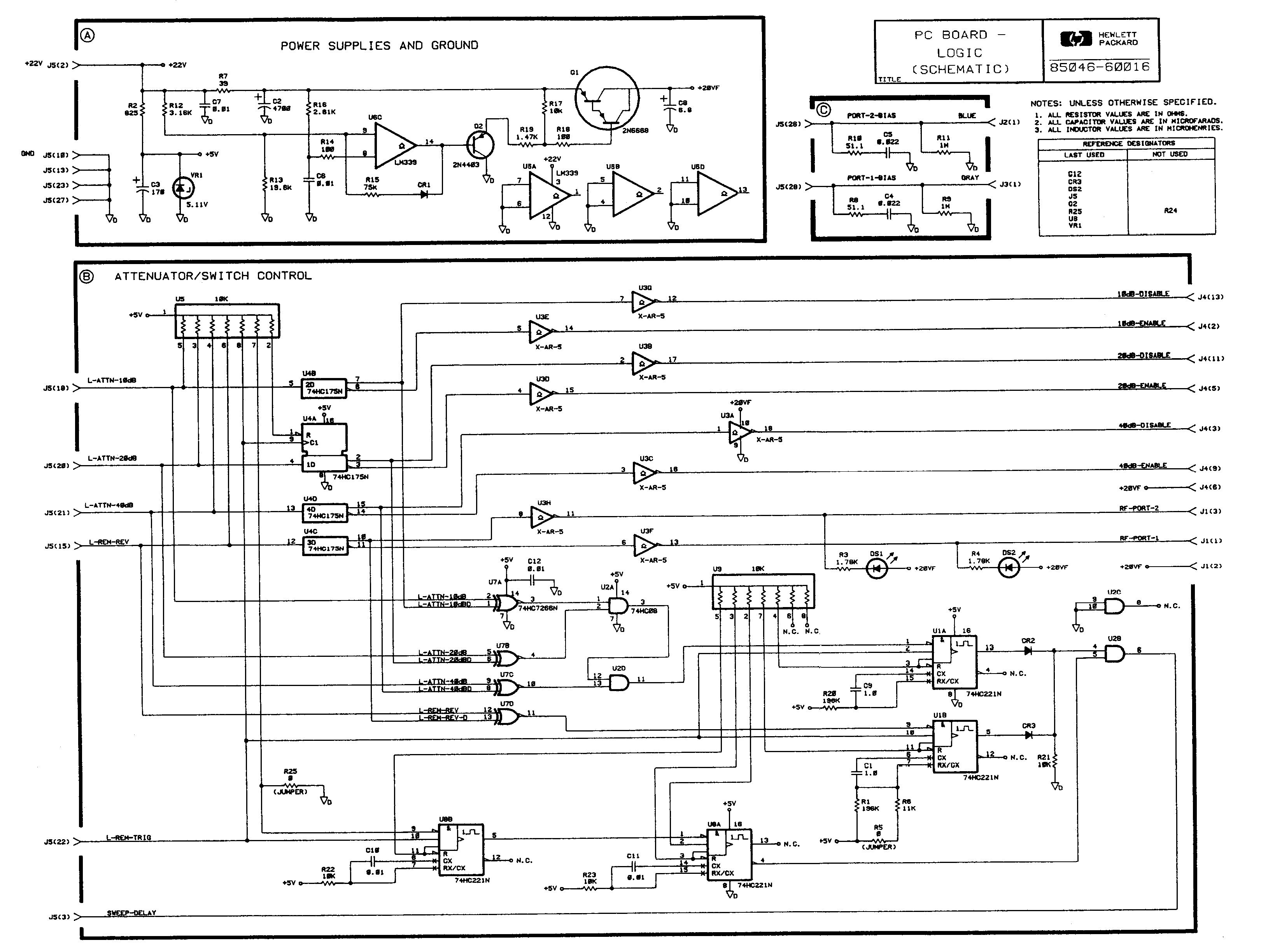
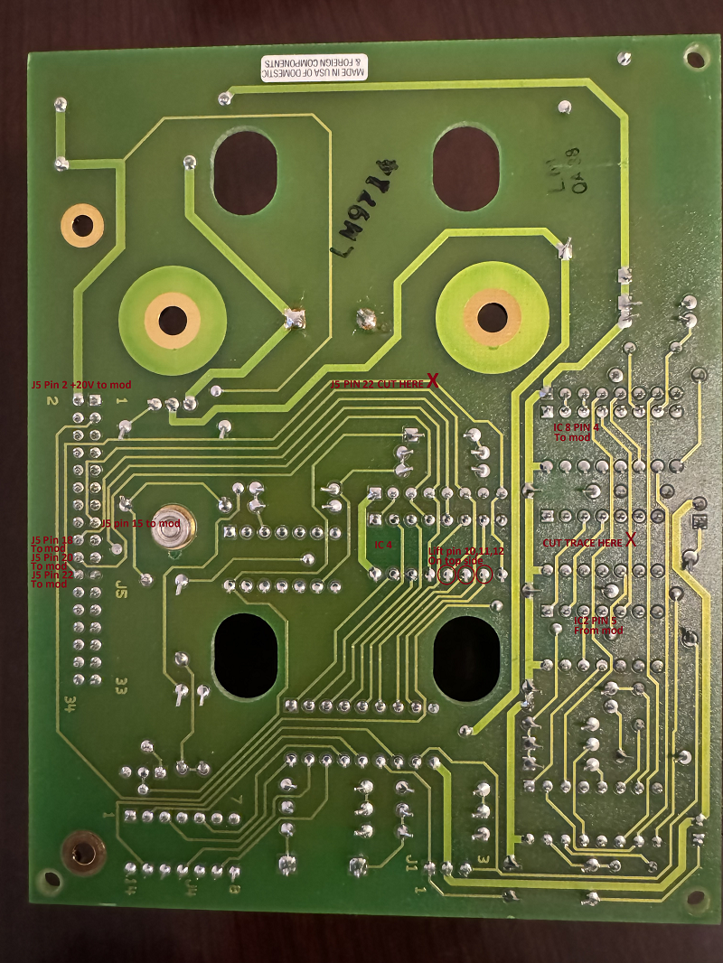
The bottom of an unmodified board is shown below. On it, you can see all the traces that I cut and all the connections that I made to the modification circuit. Please have a look at the 85046 Logic Schematic with Mods. It shows all the circuit changes made and all the connection points to the added circuit board.
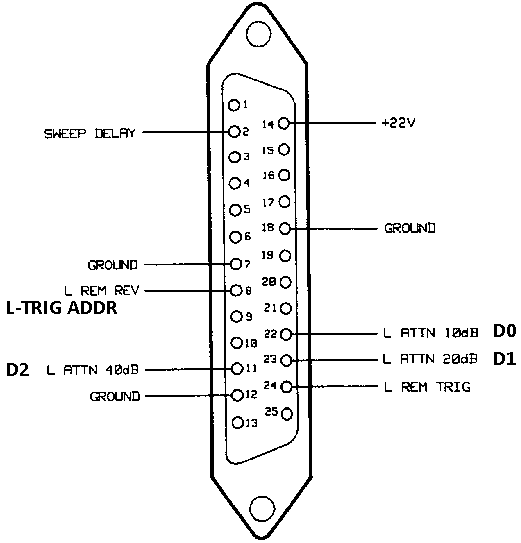
The Attenuator signals from the Instrument have 2 functions. They are the data inputs to the upper and lower latches. The L-REM REV line changes its function to L-TRIG ADDR. The lower latch did not exist in the 85046 so it was added in the modification to control the RF relays. The Logic circuit composed of U1, a 74LS00 QUAD NAND gate, is used as a decoder because I needed a fast device that would not mind a 10 nS trigger pulse from the instument. I had this in my junk box, but a 74HC00 would work as well and consume less power. The gate array decodes the Upper Latch and Lower Latch signals in the modification circuit. Looking at the Logic Schematic for the 85047, you can see a similar circuit used there to decode the L-TRIG ADD and L-REM TRIG signals using the following truth table.
|
|
|
Trigger Address |
|
Signal |
J1 pin |
Data |
High (latch) |
Low (latch) |
D0 |
22 |
H |
10 Db disable |
Doubler On |
|
|
L |
10 Db enable |
Doubler Off |
D1 |
23 |
H |
20 Db disable |
F/R fwd (drive port 1) |
|
|
L |
20 Db enable |
F/R rev (drive port 2) |
D2 |
24 |
H |
40 Db disable |
TTL output low (unused in this mod) |
|
|
L |
40 Db enable |
TTL output high |
The important difference here is the Doubler control. This modification lets us control a doubler by the instrument in a normal way just as if the test set was an 85047. The 8753C Network analyzer can’t tell the difference between this and a real 85047.
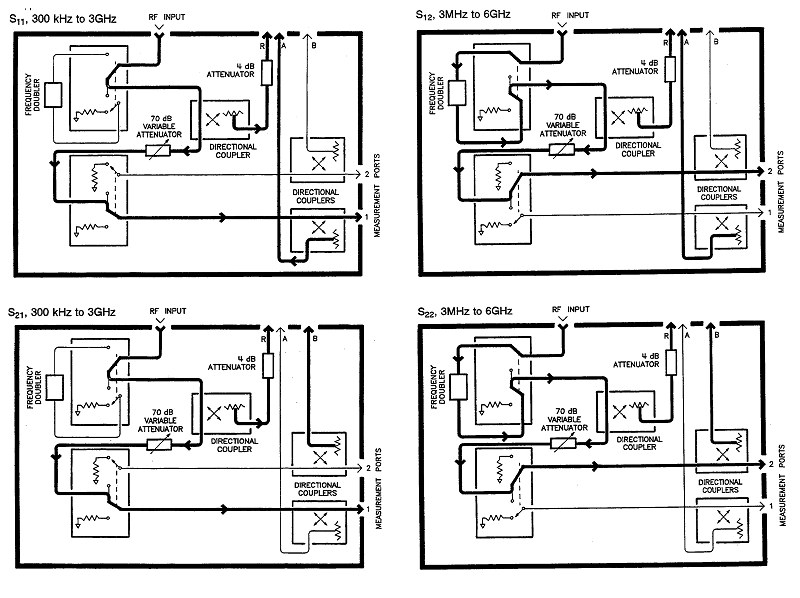
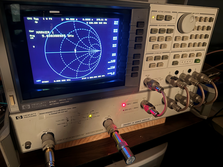
The limits of this modification depend on the RF path. My sample ports calibrate all the way to 6GHZ. I can tune filters and antennas from .3 to 6000 MHz I am guessing, but I think most 85046 units will probably have good enough RF components to calibrate out to 6 GHZ. The RF path becomes the same as an 85047 test set after modification. The RF path is shown here.
Once all the RF parts are installed and the logic circuit has been added and incorporated within the unit, all that’s left is to drill some little holes in the front panel and install a couple of LEDs. I picked a red one for 6GHZ and a green one for 3GHZ. Here is a look at my final project outside and inside.
In summery, This project was done mostly because of my love of test equipment, and for making electronic/electrical devices do more than they are supposed to do. It is published for educational purposes only. The specifications you get after this modification probably will not meet the original specs of an actual 85047 unit. However, it will be very useful above 3 GHZ. In all actuality, purchasing an actual 85047 may be more practical if you are patient and wait for one on eBay that can be had for a good price. Alternately, you could purchase a logic board out of a parted out 85047 unit and wire it into an 85046 unit. Then, buy a doubler and a 4 port switch to complete the modification.
Questions? Comments? I would love to hear from you. <Charles Singleton> support@singletone.com